
Understanding the ADC0804 Analog-to-Digital Converter
Explore the ADC0804 analog-to-digital converter, its features, pin configuration, and circuit assembly for effective signal conversion.
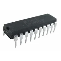
Analog-to-digital converters (ADCs) are essential components that transform analog signals into digital values. Among the various models available, the ADC0804 stands out due to its affordability and ease of use. This article delves into the ADC0804, exploring its features and operational modes.
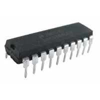
The ADC0804 is a classic ADC that operates with a variety of parameters, including conversion speed, the number of analog inputs, precision, and operating voltage. While some high-speed ADCs can be quite expensive, the ADC0804 offers a budget-friendly solution for many applications.
One of the simplest ways to utilize the ADC0804 is by setting it to free-running mode. In this mode, the ADC continuously converts signals without the need for external control. However, it also supports several controlled operation modes where the user can specify when to convert using the READ pin and when to output data via the WRITE pin.
Pin Configuration:
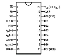
The ADC0804 features several important pins:
- CS: Chip Select, used to select which chip to activate when multiple chips are present. It remains connected to ground, as it is an active-low pin (applying 0V activates it, while +5V deactivates it).
- RD: Read, updates the 8 output pins.
- WR: Write, connected to ground and remains active continuously, allowing for uninterrupted conversion.
- CLK IN and CLK R: These pins set the chip’s frequency (internal clock).
- INTR: Interrupt pin, set to high by the chip when conversion is complete.
- Vin + and -: Analog input pins.
- Vref/2: Reference voltage.
- VCC and GND: Power supply pins.
- DB: The 8 data output pins, corresponding to the 8-bit resolution of the ADC.
Circuit Assembly:
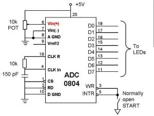
In the circuit, a 10k potentiometer (POT) is used to adjust the input signal. The clock (CLK) is connected to a resistor-capacitor (RC) network, determining the internal clock frequency. The calculation for the RC time constant is as follows:
RC = 10000 × 0.000000000150 = 0.00000150 seconds
Thus, the clock frequency is:
1/RC = 1/0.00000150 = 666 kHz
With the CS and RD pins connected to ground, they remain active at all times. The WR and INTR pins are interconnected, allowing the INTR signal, activated by the chip, to control the WR pin autonomously. This setup enables the ADC to perform continuous conversions without interruption, achieving a conversion speed of 10K samples per second.